高速TaA=10納秒
■低有功功率ICC=90 mA,100兆赫
■低CMOS待機電流Isb2=20 mA(典型)工作電壓為2.2 V至3.6 V
■1.0 V數據保留
■取消選擇時自動斷電TTL兼容輸入和輸出
■具有CE1和CE2功能的輕松內存擴展
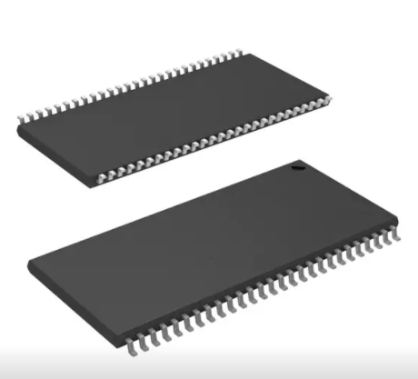
■提供無鉛54針TSOP II和48球VFBGA。包裝
■提供雙芯片啟用選項

功能描述
C7C1061GN30是一個高性能CMOS Static Ram
按16比特計,組織編號為1048576。
To write to the device,take chip enables(CE1 low and ce2)
High)and write enable(we)input low.If byte low enable
(ble)is low,they data from I/o pins(I/O through I/O7),is
Written into the location specified on the address pins(A0 through)
頁:1If byte high enable(BHE)is low,they data from I/o pins
(I/O8 through I/15)is written into the location specified on the
Address Pins(A0 through A19).
To read from the Device,Take Chip Enables(CE1 low and CE2)
High)and output enable(OE)low while forcing the write
Enable(we)high.If byte low enable(ble)is low,then data
From the memory location specified by the address pins appears
On I/O to I/O7.If byte high enable(BHE)is low,they data from
Memory Appeals on I/O8 to I/15.See truth table on page 12
閱讀和寫作方式的完整描述。
The input or output pins(I/O through I/15)are placed in a high
當惡魔被攝取時(CE1 high/ce2)
Low,the outputs are disabled(OE High),the BHE and able
Are disabled(BHE,a ble high),or during a write operation(CE1)
Low,CE2 high,and we low)


