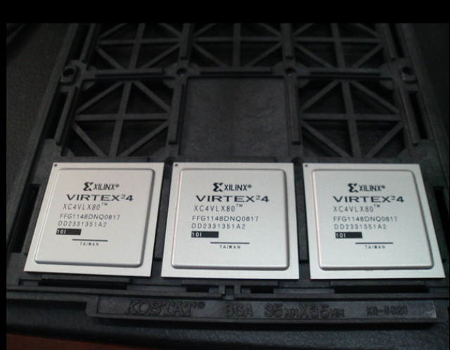
The Virtex®-5 family provides the newest most powerful features in the FPGA market. Using the second generation ASMBL (Advanced Silicon Modular Block) column-based architecture, the Virtex-5 family contains five distinct platforms (sub-families), the most choice offered by any FPGA family. Each platform contains a different ratio of features to address the needs of a wide variety of advanced logic designs. In addition to the most advanced, high-performance logic fabric, Virtex-5 FPGAs contain many hard-IP system level blocks, including powerful 36-Kbit block RAM/FIFOs, second generation 25 x 18 DSP slices, SelectIO technology with built-in digitallycontrolled impedance, ChipSync source-synchronous interface blocks, system monitor functionality, enhanced clock management tiles with integrated DCM (Digital Clock Managers) and phase-locked-loop (PLL) clock generators, and advanced configuration options. Additional platform dependant features include power-optimized high-speed serial transceiver blocks for enhanced serial connectivity, PCI Express® compliant integrated Endpoint blocks, tri-mode Ethernet MACs (Media Access Controllers), and high-performance PowerPC® 440 microprocessor embedded blocks. These features allow advanced logic designers to build the highest levels of performance and functionality into their FPGA-based systems. Built on a 65-nm state-of-the-art copper process technology, Virtex-5 FPGAs are a programmable alternative to custom ASIC technology. Most advanced system designs require the programmable strength of FPGAs. Virtex-5 FPGAs offer the best solution for addressing the needs of high-performance logic designers, high-performance DSP designers, and high-performance embedded systems designers with unprecedented logic, DSP, hard/soft microprocessor, and connectivity capabilities.
Key Features Virtex-5 FXT: High-performance embedded systems with advanced serial connectivity FXT devices are footprint compatible in the same package using adjustable voltage regulators Most advanced, high-performance, optimal-utilization, FPGA fabric Real 6-input look-up table (LUT) technology Dual 5-LUT option Improved reduced-hop routing 64-bit distributed RAM option SRL32/Dual SRL16 option Powerful clock management tile (CMT) clocking Digital Clock Manager (DCM) blocks for zero delay buffering, frequency synthesis, and clock phase shifting PLL blocks for input jitter filtering, zero delay buffering, frequency synthesis, and phase-matched clock division 36-Kbit block RAM/FIFOs True dual-port RAM blocks Enhanced optional programmable FIFO logic Programmable - True dual-port widths up to x36 - Simple dual-port widths up to x72 Built-in optional error-correction circuitry Optionally program each block as two independent 18-Kbit blocks High-performance parallel SelectIO technology 1.2 to 3.3V I/O Operation Source-synchronous interfacing using ChipSync™ technology Digitally-controlled impedance (DCI) active termination Flexible fine-grained I/O banking High-speed memory interface support Advanced DSP48E slices 25 x 18, two’s complement, multiplication Optional adder, subtracter, and accumulator Optional pipelining Optional bitwise logical functionality Dedicated cascade connections Flexible configuration options SPI and Parallel FLASH interface Multi-bitstream support with dedicated fallback reconfiguration logic Auto bus width detection capability System Monitoring capability on all devices On-chip/Off-chip thermal monitoring On-chip/Off-chip power supply monitoring JTAG access to all monitored quantities Integrated Endpoint blocks for PCI Express Designs Tri-mode 10/100/1000 Mb/s Ethernet MACs RocketIO GTX transceivers 150 Mb/s to 6.5 Gb/s TXT and FXT Platforms PowerPC 440 Microprocessors FXT Platform only RISC architecture 7-stage pipeline 32-Kbyte instruction and data caches included Optimized processor interface structure (crossbar) 65-nm copper CMOS process technology 1.0V core voltage High signal-integrity flip-chip packaging available in standard or Pb-free package options


